
Bow, warp, TTV & quality inspection of wafers in ultra-short cycle times
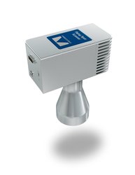
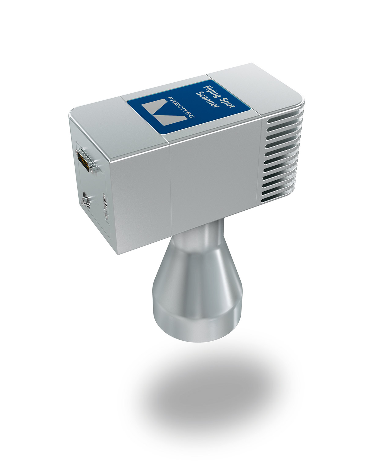
The Flying Spot Scanner (FSS) 310 uniquely combines OCT with wide field-of-view scanning, and solves the problem that ultra-precise measuring systems are normally very slow and extremely expensive.
The FSS 310 has a flexible, fast-moving measurement point within the field of view which enables a ROI inspection in ultra-short cycle times – without compromising accuracy. This device measures the total thickness variation (TTV), bow, warp and voids of an entire 12-inch wafer in a single scan.


Advantages
- High-speed, non-contact ROI inspection
With a huge scan area of 310 mm, the FSS 310 checks a 12-inch wafer for TTV, bow, warp and voids in standard applications in less than 40 seconds, which enables a throughput of over 70 wafers per hour (including handling time). Thanks to the in-built scanning system, long paths of linear axes are replaced by short rotary movements, which significantly reduces measuring times and does away with the need for a precision axis. - Ease of use
The FSS 310 and the optical sensor CHRocodile 2 IT form a standalone package that is easily integratable in in- and offline systems. Only a single connection to the CHRocodile 2 IT controller is needed to carry out a customized scan procedure with the FSS 310. Multiple software interfaces and tools enable you to easily set up your application. The list of defined measurement tasks is then stored on the optical sensor, which also controls the probe before a software visualizes the results. - Great flexibility in inline inspection
The FSS 310 allows measurements from just one side of a wafer as it penetrates all important semiconductor materials – apart from metal – and even measures objects behind or on the rear side of a wafer. Through ultra-fast ROI inspection with no additional axis or precision hardware needed, it can be easily integrated into automated or inline applications with no interruption of production thanks to the ultra-short cycle times. - Broad applicability
In combination with devices from the CHR 2 IT family, the fully variable scan trajectories programmable by the user enable thickness and distance measurement of Si, doped Si, GaAs and SiC wafers. The FSS not only measures bow, warp and TTV but also detects voids on wafers, performs thickness measurements of semiconductor component coatings (e.g. partial foliation of wafers) as well as measuring the bow of individual dies on wafers prior to further processing.
Technical data
- Measured values: Thickness, distance
- Measuring rate: Up to 70,000 Hz
- Measuring range: Depends on CHRocodile 2 IT sensor
- Lateral resolution: 20 µm (CHRocodile 2 IT DW)
- Working distance: 150 mm
- Max. jump speed: 10 m/s
- Scan area (diameter): 310 mm
- Numerical aperture: 0.018
- Measurement angle to surface: 90° +/- 1°
- Dimensions (h x d) with optics: 742 mm x 360 mm
We need your consent to load the form!
We use Marketing Cloud Account Engagement (Pardot) Forms to embed content that may collect data about your activity. Please review the details and click in the Pardot box to accept the service and see the content. If the form is not displayed correctly, please click once more on Download the data sheet now.