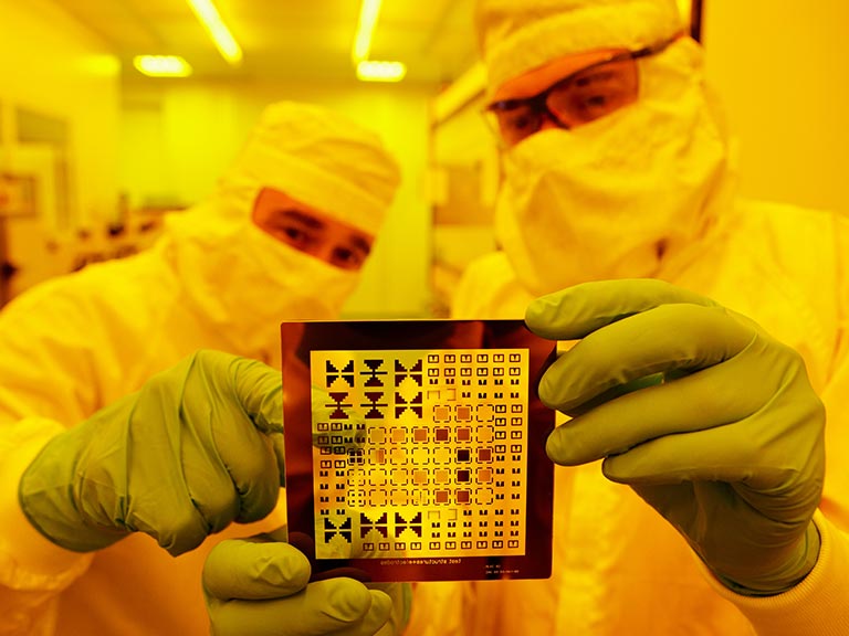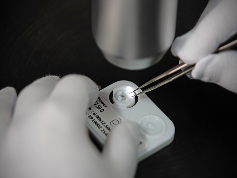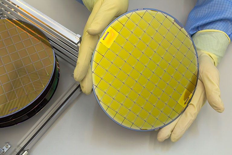
Semiconductor industry
State-of-the-art wafer inspection
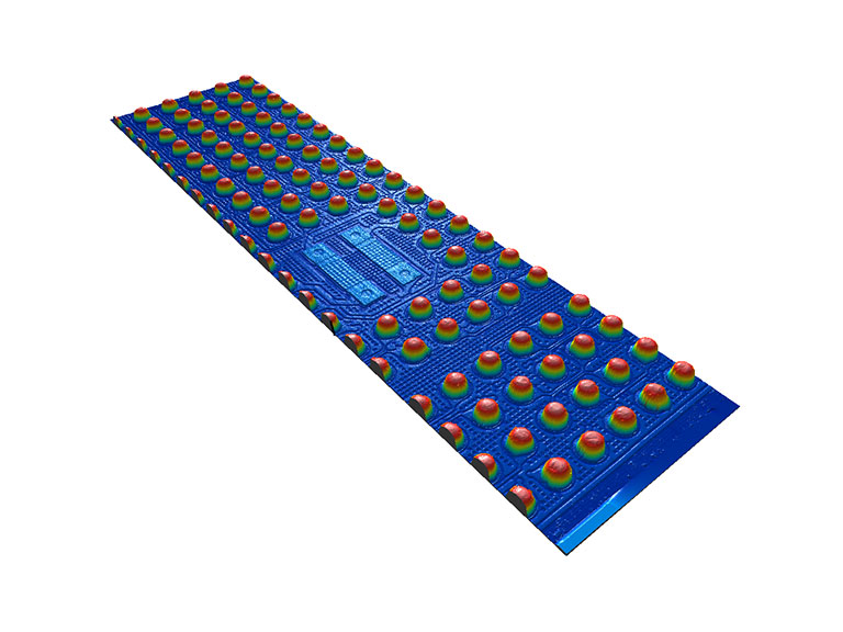
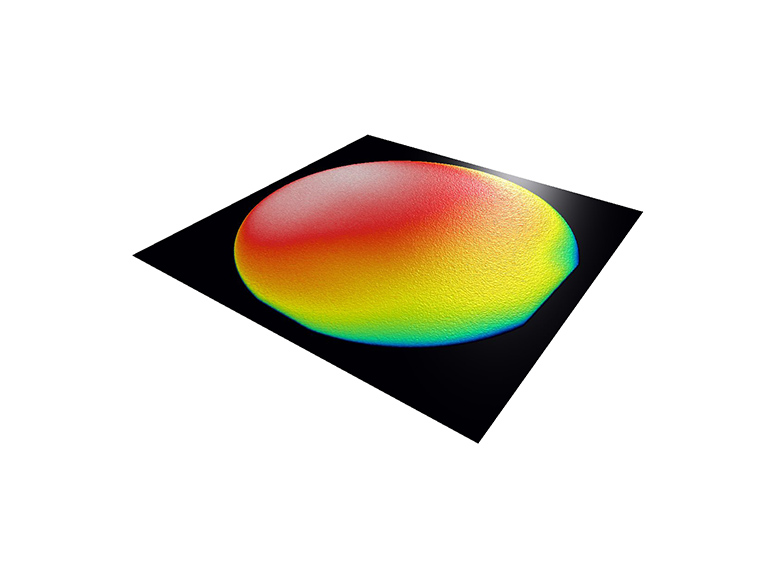
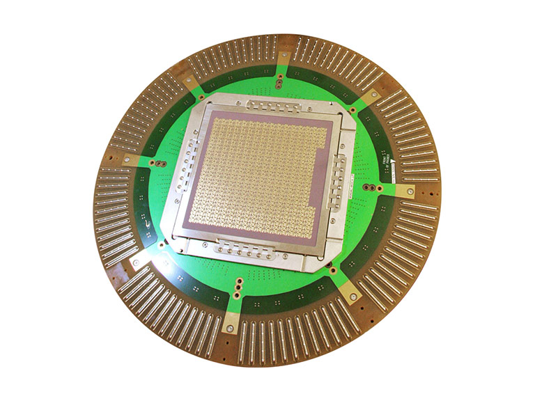
Our non-destructive optical measurement technology offers ultra-precise measurement and analysis of semiconductor chips (wafers). The high-resolution 3D data these semiconductor sensors collect allows the topography of the circuits to be examined in the necessary detail.
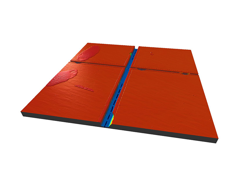
Our CHRomatic confocal line sensor CHRocodile CLS measure up to 192 measuring points in close proximity so that the optical probe covers a much larger area in a given time than a conventional point sensor.
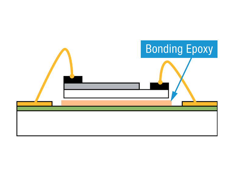
Our CHRocodile 2 IT series carries out thickness measurements of wafers, glues, and coatings at high speed to enable higher semiconductor throughput coupled with more accurate and repeatable product quality.
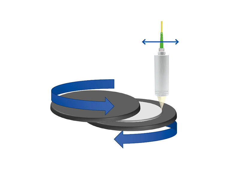
These reliable high-speed tools measure endpoint thicknesses in situ during workplace treatment in CMP, back grinding, and spin etching. In the final analysis, optical monitoring makes semiconductor production processes more efficient, which reduces material waste.