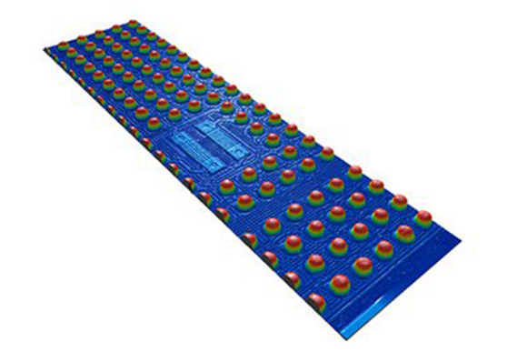
Full-field, non-contact optical mapping for wafer topography and bow control
This Photonics article highlights how advanced metrology is moving to the frontline of semiconductor manufacturing, enabling tighter process control at advanced nodes. It underscores the importance of high-precision, in-line measurement solutions-such as those from Precitec 3D Metrology-toensure yield, speed, and reliability in modern fabs. The full article can be read by clicking on this link.
Full-field, non-contact optical mapping for wafer topography and bow control
This year, Precitec is once again taking responsibility and providing targeted support for social institutions and regional projects. 💙
One of our…

The Explorer project began over two years ago with a clear vision: to get children and young people interested in nature, people and technology and to…

Our participation in LASER World of PHOTONICS 2025 was a complete success. Our stand met with a great response, interest in our technologies was…

On Wednesday, May 14, 2025, the time had come again. 25 running enthusiasts from Precitec took part in this year's "BW-RUNNING" company run in Bühl.
…

Artificial intelligence is a driver of innovation in photonics. Whether in industrial production, quality assurance, medicine and research or…
The Fraunhofer Institute for Solar Energy Systems ISE and Precitec are working together on the "Quaze" research project to develop an optical test…

We are pleased to present our brand new webshop - optimized for easier and more efficient ordering of spare parts for laser systems. Thanks to a…

We are delighted to be supporting the children's hospice in Karlsruhe, Germany again this year with a Christmas donation. It does valuable work by…
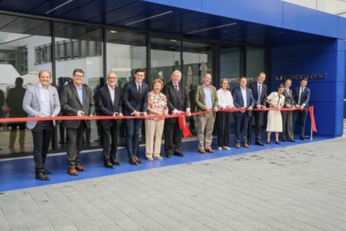
Another step forward: For a few weeks now, we have been able to work in our new, modern workplaces. This has resulted in improved collaboration and…